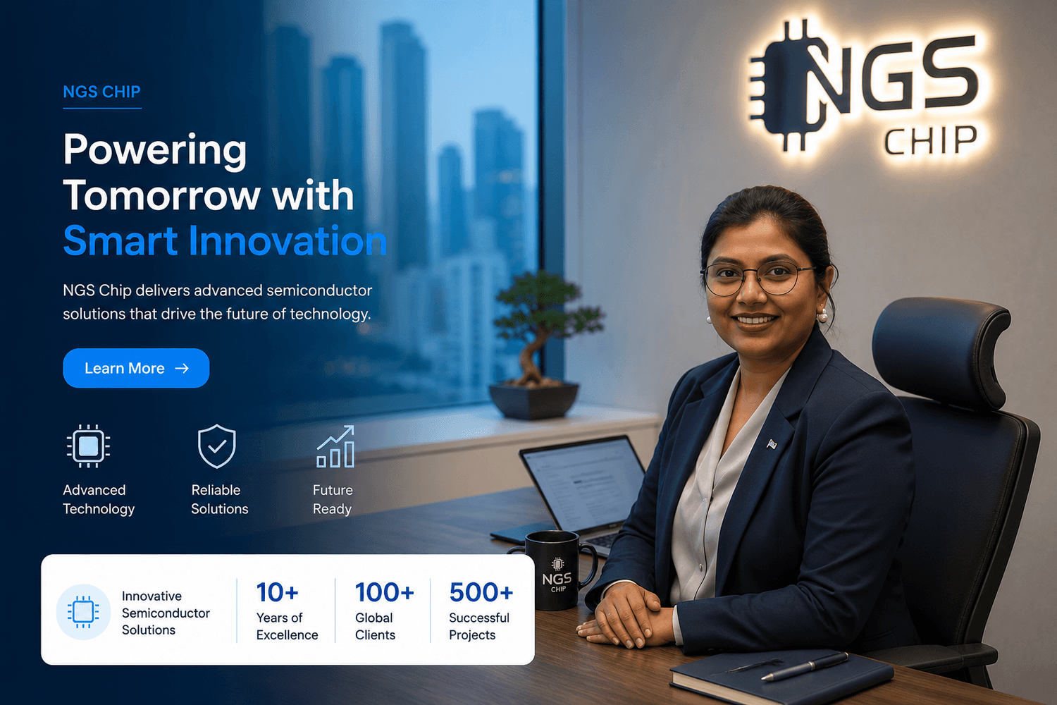
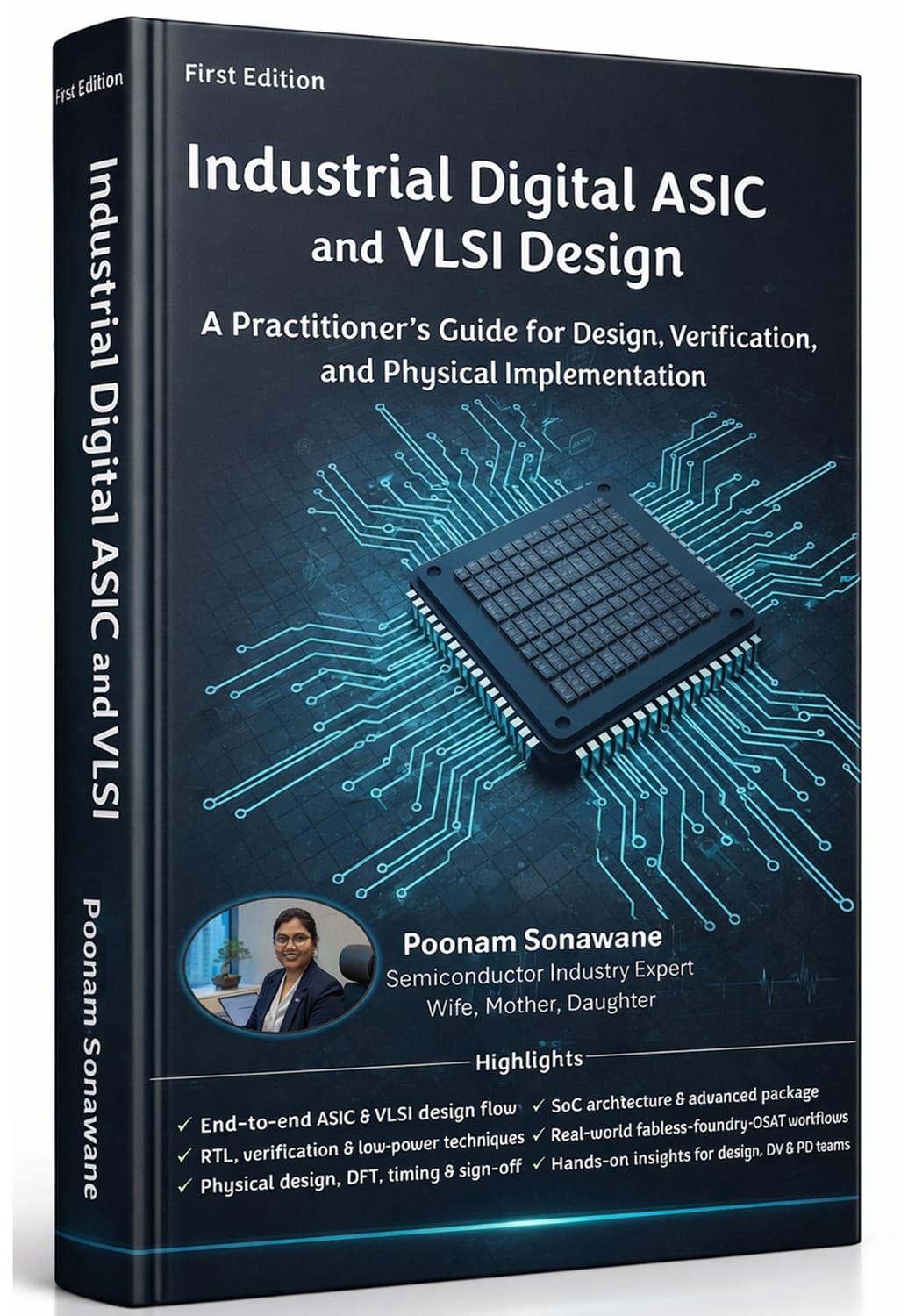
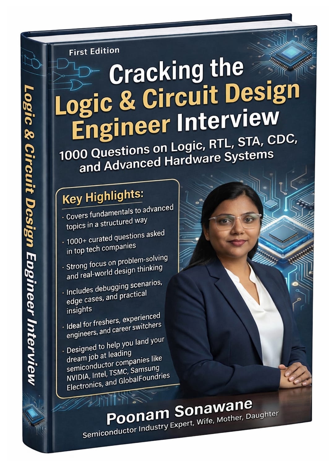
SEMICONDUCTOR EDUCATION • VLSI • AI CHIPS • FABRICATION
Master Semiconductor Chip Design & Fabrication with NGS Chip
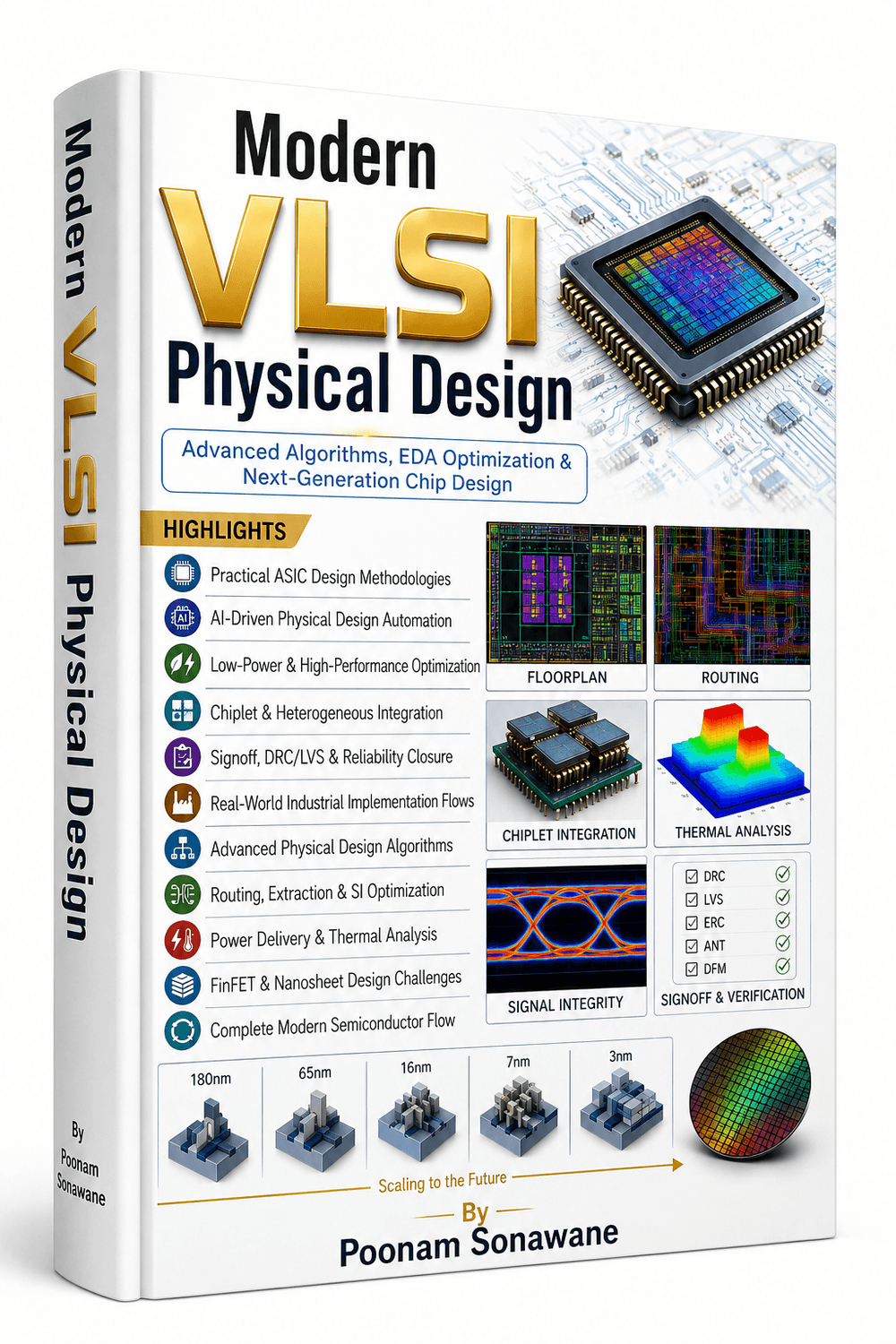
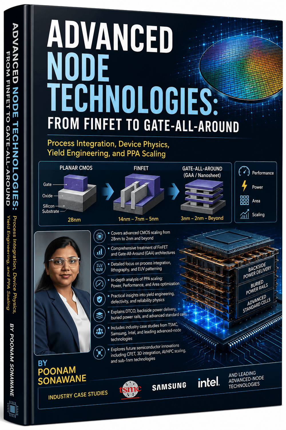
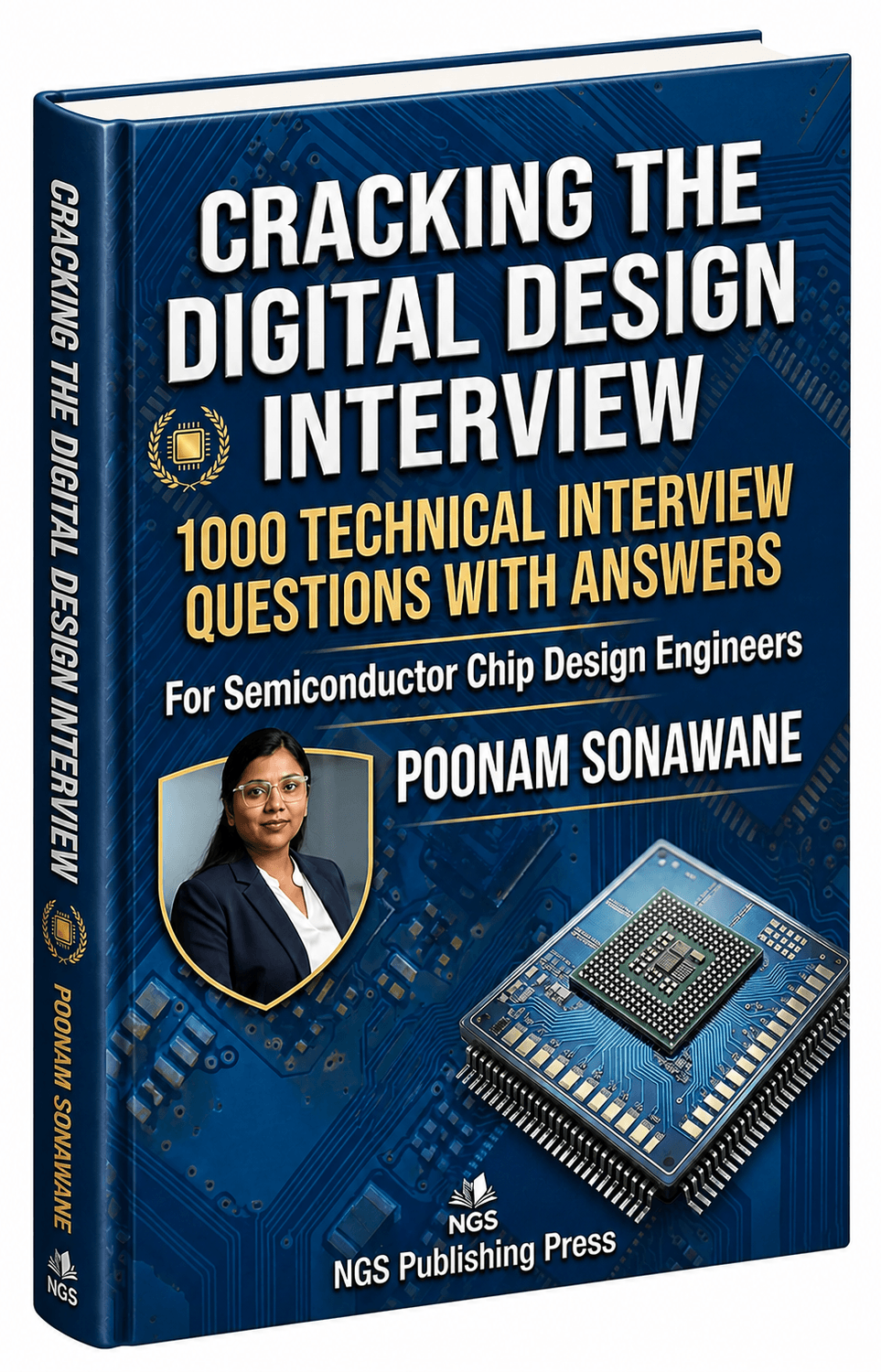
Premium eBooks, Industry-Level Courses, and Advanced Training in VLSI, Physical Design, AI Chips & Semiconductor Manufacturing


20k+
Semiconductor Community
50+
Technical Interview Resources
2-3x
Higher Job Opportunities
How WE can help YOU!
We understand the challenges that come with running an e-commerce business. From attracting new customers to retaining existing ones, there are countless factors that can impact your success in the digital marketplace.
That's where we come in.
Our team of expert e-commerce consultants has years of experience helping businesses just like yours overcome these challenges and achieve their goals.
Expertise
We stay up-to-date on the latest trends and best practices in the industry and are committed to providing you with the highest level of expertise and support.
Customized solutions
We take a customized approach to our consulting services, tailoring our strategies to meet the specific needs and goals of your business.
Results-driven
We take a data-driven approach to our consulting services, using analytics and metrics to measure the success of our strategies and make informed decisions.
Long-term partnership
We're committed to building long-term partnerships with our clients, working closely with you to achieve sustained growth and success in the marketplace.
We're committed to helping you achieve
Your Ecommerce Goals!
Just Click on The Button Below and Start Today!
The Solutions We Provide

Website Optimization
Our team will conduct a thorough analysis of your website to identify areas for improvement.

Digital Marketing
We'll help you develop and implement a data-driven digital marketing strategy.

Customer Retention
Keeping your existing customers happy is just as important as attracting new ones.

Data Analysis
Detailed reports and insights on your website and marketing performance.

Platform Selection
We can help you choose the right e-commerce platform for your business.

Business Growth
Our goal is to help you achieve sustained growth and success in the e-commerce marketplace.

100% RISK FREE INVESTMENT
Our Guarantee
We are committed to providing our customers with the highest quality products and services. satisfied with your purchase.
If for any reason you are not completely satisfied with a product or service you purchase from us, simply contact us within 2 days and we will refund your money or offer a replacement.